Introduction Embedded systems are literally everywhere in our society today. A simple definition of an embedded system is a special-purpose computer system that is part of a larger system or machine with the intended purpose of providing monitoring and control services to that system or machine. The typical embedded system starts running some special purpose application as soon as it is turned on and will not stop until it is turned off. Virtually every electronic device designed and produced today is an embedded system. A short list of embedded system examples include:
Alarm clocks
Automatic teller machines
Cellular phones
Computer printers
Antilock brake controllers
Microwave ovens
Inertial guidance systems for missiles
DVD players
Personal digital assistants (PDAs)
Programmable logic controllers
(PLC) for industrial automation and
monitoring
Portable music players
Maybe even your toaster...
Embedded systems can contain many different types of devices including microprocessors, microcontrollers, DSPs, RAM, EPROMs, FPGAs, A/Ds, D/As, and I/O. These various devices have traditionally communicated with each other and the outside world using wide parallel buses. Today, however, more and more of the building blocks used in embedded system design are replacing these wide parallel buses with serial buses for the following reasons:
Less board space required due to fewer signals to route
Lower cost
Lower power requirements
Fewer pins on packages
Embedded clocks
Differential signaling for better noise immunity
Wide availability of components using standard
serial interfaces
While serial buses provide a number of advantages, they also pose some significant challenges to an embedded system designer due simply to the fact that information is being transmitted in a serial fashion rather than parallel. This application note discusses common challenges for embedded system designers and how to overcome them using capabilities found in the MSO/DPO SeriesMSO/DPO4000, DPO3000 and MSO/DPO2000 Seriesoscilloscopes.
Parallel vs. Serial
With a parallel architecture, each component of the bus has its own signal path. There may be 16 address lines, 16 data lines, a clock line and various other control signals. Address or data values sent over the bus are transferred at the same time over all the parallel lines. This makes it relatively easy to trigger on the event of interest using either the State or Pattern triggering found in most oscilloscopes and logic analyzers. It also makes it easy to understand at a glance the data you capture on either the oscilloscope or logic analyzer display.
For example, in Figure 1 we’ve used a logic analyzer to acquire the clock, address, data and control lines from a microcontroller. By using a state trigger, we’ve isolated the bus transfer we’re looking for. To “decode” what’s happening on the bus, all we have to do is look at the logical state of each of the address, data, and control lines. With a serial bus all this information must be sent serially on the same few conductors (sometimes one). This means that a single signal may include address, control, data, and clock information. As an example, look at the Controller Area Network (CAN) serial signal shown in Figure 2.
Figure 1. Logic Analyzer acquisition of a microcontroller’s clock, address bus, data bus and control lines.
This message contains a start of frame, an identifier (address), a data length code, data, CRC, and end of frame as well as a few other control bits. To further complicate matters, the clock is embedded in the data and bit stuffing is used to ensure an adequate number of edges for the receiving device to lock to the clock. Even to the very trained eye, it would be extremely difficult to quickly interpret the content of this message. Now imagine this is a faulty message that only occurs once a day and you need to trigger on it. Traditional oscilloscopes and logic analyzers are simply not well equipped to deal with this type of signal.
Even with a simpler serial standard such as I2C, it is still significantly harder to observe what is being transmitted over the bus than it is with a parallel protocol.
I2C uses separate clock and data lines, so at least in this case you can use the clock as a reference point. However, you still need to find the start of the message (data going low while the clock is high), manually inspect and write down the data value on every rising edge of the clock, and then organize the bits into the message structure.
It can easily take a couple of minutes of work just to decode a single message in a long acquisition and you have no idea if that’s the message you are actually looking for. If it’s not, then you need to start this tedious and error-prone process over on the next one. It would be nice to just trigger on the message content you are looking for, however the state and pattern triggers you’ve used for years on scopes and logic analyzers won’t do you any good here. They are designed to look at a pattern occurring at the same time across multiple channels. To work on a serial bus, their trigger engines would need to be tens to hundreds of states deep (one state per bit). Even if this trigger capability existed, it would not be a fun task programming it state-by-state for all these bits. There has to be a better way!
With the MSO/DPO SeriesMSO/DPO4000, DPO3000 and MSO/DPO2000 Seriesthere is a better way. The following sections highlight how the MSO/DPO Series can be used with some of the most common low-speed serial standards used in embedded system design.
I2C
Background I2C, or “I squared C”, stands for Inter-Integrated Circuit. It was originally developed by Philips in the early 1980s to provide a low-cost way of connecting controllers to peripheral chips in TV sets, but has since evolved into a worldwide standard for communication between devices in embedded systems. The simple two-wire design has found its way into a wide variety of chips like I/O, A/Ds, D/As, temperature sensors, microcontrollers and microprocessors from numerous leading chipmakers including: Analog Devices, Atmel, Infineon, Cyprus, Intel, Maxim, Philips, Silicon Laboratories, ST Microelectronics, Texas Instruments, Xicor, and others.
How It Works I2C’s physical two-wire interface is comprised of bi-directional serial clock (SCL) and data (SDA) lines. I2C supports multiple masters and slaves on the bus, but only one master may be active at a time. Any I2C device can be attached to the bus allowing any master device to exchange information with a slave device. Each device is recognized by a unique address. A device can operate as either a transmitter or a receiver, depending on its function. Initially, I2C only used 7-bit addresses, but evolved to allow 10-bit addressing as well. Three bit rates are supported: 100 kb/s (standard mode), 400 kb/s (fast mode), and 3.4 Mb/s (high-speed mode). The maximum number of devices is determined by a maximum capacitance of 400 pF or roughly 20-30 devices.
The I2C standard specifies the following format in Figure 4:
Start indicates the device is taking control of the bus and that a message will follow.
Address a 7 or 10 bit number representing the address of the device that will either be read from or written to.
R/W Bit one bit indicating if the data will be read from or written to the device.
Ack one bit from the slave device acknowledging the master’s actions. Usually each address and data byte has an acknowledge, but not always.
Data an integer number of bytes read from or written to the device.
Stop indicates the message is complete and the master has released the bus.
There are two ways to group I2C addresses for decoding: in 7-bits plus a read or write (R/W) bit scheme, and in 8-bits (a byte) where the R/W bit is included as part of the address. The 7-bit address scheme is the specified I2C Standard followed by firmware and software design engineers. But many other engineers use the 8-bit address scheme. The MSO/DPO Series oscilloscopes can decode data in either scheme.
Figure 4. I2C message structure.
Working with I2C With the DPOxEMBD serial triggering and analysis application module, the MSO/DPO Series becomes a powerful tool for embedded system designers working with I2C buses. The front panel has Bus buttons that allow the user to define inputs to the scope as a bus. The I2C bus setup menu is shown in Figure 5.
Figure 5. I2C bus set-up menu.
By simply defining which channels clock and data are on, along with the thresholds used to determine logic ones and zeroes, you’ve enabled the oscilloscope to understand the protocol being transmitted across the bus. With this knowledge, the oscilloscope can trigger on any specified messagelevel information and then decode the resulting acquisition into meaningful, easily interpreted results. Gone are the days of edge triggering, hoping you acquired the event of interest, and then manually decoding message after message while looking for the problem.
As an example, consider the embedded system in Figure 6. An I2C bus is connected to multiple devices including a CPU, an EEPROM, a fan speed controller, a digital to analog converter, and a couple of temperature sensors.
Figure 6. I2C bus example.
This instrument was returned to engineering for failure analysis as the product was consistently getting too hot and shutting itself off. The first thing to check is the fan controller and the fans themselves, but they both appear to be working correctly. The next thing to check for is a faulty temperature sensor. The fan speed controller polls the two temperature sensors (located in different areas of the instrument) periodically and adjusts the fan speed to regulate internal temperature. You’re suspicious that one or both of these temperature sensors is not reading correctly. To see the interaction between the sensors and the fan speed controller, we simply need to connect to the I2C clock and data lines and set up a bus on the MSO/DPO Series. We know that the two sensors are addresses 18 and 19 on the I2C bus, so we decide to set up a trigger event to look for awrite to address 18 (the fan speed controller polling the sensor for the current temperature). The triggered acquisition is shown in the screenshot Figure 7.
Figure 7. I2C address and data bus waveform decoding.
In this case, channel 1 (yellow) is connected to SCLK and channel 2 (cyan) to SDA. The purple waveform is the I2C bus we’ve defined by inputting just a few simple parameters to the oscilloscope. The upper portion of the display shows the entire acquisition. In this case we’ve captured a lot of bus idle time with a burst of activity in the middle which we’ve zoomed in on. The lower, larger portion of the display is the zoom window. As you can see, the oscilloscope has decoded the content of each message going across the bus. Buses on the MSO/DPO Series use the colors and marks in Table 1 to indicate important parts of the message.
Table 1. Bus conditions.
Taking a look at the acquired waveforms, we can see that the oscilloscope did indeed trigger on a Write to address 18 (shown in the lower left of the display). In fact, the fan speed controller attempted to write to address 18 twice, but in both cases it did not receive an acknowledge after attempting to write to the temperature sensor. It then checked the temperature sensor at Address 19 and received back the desired information. So, why isn’t the first temperature sensor responding to the fan controller? Taking a look at the actual part on the board we find that one of the address lines isn’t soldered correctly. The temperature sensor was not able to communicate on the bus and the unit was overheating as a result. We’ve managed to isolate this potentially elusive problem in a matter of a couple minutes due to the I2C trigger and bus decoding capability of the MSO/DPO Series.
In the example in Figure 7 we triggered on a write, but the MSO/DPO Series’ powerful I2C triggering includes many other capabilities:
Start triggers when SDA goes low while SCL is high.
Repeated Start triggers when a start condition occurs without a previous stop condition. This is usually when a master sends multiple messages without releasing the bus.
Stop triggers when SDA goes high while SCL is high.
Missing Ack slaves are often configured to transmit an acknowledge after each byte of address and data. The oscilloscope can trigger on cases where the slave does not generate the acknowledge bit.
Address triggers on a user specified address or any of the pre-programmed special addresses including General Call, Start Byte, HS-mode, EEPROM, or CBUS. Addressing can be either 7 or 10 bits and is entered in binary or hex.
Data triggers on up to 12 bytes of user specified data values entered in either binary or hex.
Address and Data this allows you to enter both address and data values as well as read vs. write to capture the exact event of interest.
These triggers allow you to isolate the particular bus traffic you’re interested in, while the decoding capability enables you to instantly see the content of every message transmitted over the bus in your acquisition.
SPI
Background The Serial Peripheral Interface bus (SPI) was originally developed by Motorola in the late 1980s for their 68000 series micro-controllers. Due to the simplicity and popularity of the bus, many other manufacturers have adopted the standard over the years. It is now found in a broad array of components commonly used in embedded system design. SPI is primarily used between micro-controllers and their immediate peripheral devices. It’s commonly found in cell phones, PDAs, and other mobile devices to communicate data between the CPU, keyboard, display, and memory chips.
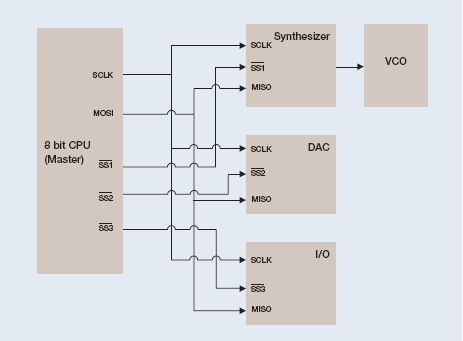
How It Works The SPI bus is a master/slave, 4-wire serial communications bus. The four signals are clock (SCLK), master output/slave input (MOSI), master input/slave output (MISO), and slave select (SS). Whenever two devices communicate, one is referred to as the "master" and the other as the “slave”. The master drives the serial clock. Data is simultaneously transmitted and received, making it a full-duplex protocol. Rather than having unique addresses for each device on the bus, SPI uses the SS line to specify which device data is being transferred to or from. As such, each unique device on the bus needs its own SS signal from the master. If there are 3 slave devices, there are 3 SS leads from the master, one to each slave as shown in Figure 8.
Figure 8. Common SPI configuration.
In Figure 8, each slave only talks to the master. However, SPI can be wired with the slave devices daisy-chained, each performing an operation in turn, and then sending the results back to the master as shown in Figure 9.
Figure 9. Daisy-chained SPI configuration.
So, as you can see, there is no “standard” for SPI implementation. In some cases, where communication from the slave back to the master is not required, the MISO signal may be left out all together. In other cases there is only one master and one slave device and the SS signal is tied to ground. This is commonly referred to as 2-wire SPI.
When an SPI data transfer occurs, an 8-bit data word is shifted out on MOSI while a different 8-bit data word is being shifted in on MISO. This can be viewed as a 16-bit circular shift register. When a transfer occurs, this 16-bit shift register is shifted 8 positions, thus exchanging the 8-bit data between the master and slave devices. A pair of registers, clock polarity (CPOL) and clock phase (CPHA) determine the edges of the clock on which the data is driven. Each register has two possible states which allows for four possible combinations, all of which are incompatible with one another. So a master/slave pair must use the same parameter values to communicate. If multiple slaves are used that are fixed in different configurations, the master will have to reconfigure itself each time it needs to communicate with a different slave.
Working with SPI The DPOxEMBD serial triggering and analysis application module enables decoding and triggering for the SPI bus. Again, using the front panel Bus buttons we can define an SPI bus by simply entering the basic parameters of the bus including which channels SCLK, SS, MOSI, and MISO are on, thresholds, and polarities (see Figure 10).
Figure 10. SPI bus setup menu.
As an example, consider the embedded system in Figure 11.
Figure 11. Synthesizer controlled via SPI.
An SPI bus is connected to a synthesizer, a DAC, and some I/O. The synthesizer is connected to a VCO that provides a 2.5 GHz clock to the rest of the system. The synthesizer is supposed to be programmed by the CPU at startup. However, something isn’t working correctly as the VCO is stuck at its rail generating 3 GHz. The first step in debugging this problem is to inspect the signals between the CPU and the synthesizer to be sure the signals are present and there are no physical connection problems, but we don’t find anything wrong. Next we decide to take a look at the actual information being transmitted across the SPI bus to program the synthesizer. To capture the information we set the oscilloscope to trigger on the synthesizer’s Slave Select signal going active and power up the DUT to capture the start up programming commands. The acquisition is shown in Figure 12.
Figure 12. Acquiring synthesizer configuration messages off the SPI bus.
Channel 1 (yellow) is SCLK, channel 2 (cyan) is MOSI and channel 3 (magenta) is SS. To help determine if we’re programming the device correctly we take a look at the data sheet for the synthesizer. The first three messages on the bus are supposed to initialize the synthesizer, load the divider ratio, and latch the data. According to the spec, the last nibble (single hex character) in the first three transfers should be 3, 0, and 1, respectively, but we’re seeing 0, 0, and 0.
Upon seeing all 0s at the end of the messages we realize we’ve made one of the most common mistakes with SPI by programming the bits in each 24-bit word in reverse order in the software. A quick change in the software results in the following acquisition and a VCO correctly locked at 2.5 GHz as shown in Figure 13.
In the example above we used a simple SS Active trigger. The full SPI triggering capability in the MSO/DPO Series includes the following types:
SS Active triggers when the slave select line goes true for a slave device.
MOSI trigger on up to 16 bytes of user specified data from the master to a slave.
MISO trigger on up to 16 bytes of user specified data from a slave to the master.
MOSI/MISO trigger on up to 16 bytes of user specified data for both master to slave and slave to master.
Again, these triggers allow you to isolate the particular bus traffic you’re interested in, while the decoding capability enables you to instantly see the content of every message transmitted over the bus in your acquisition.
RS-232
Background RS-232 is a widely-used standard for serial communication between two devices over a short distance. It is best known for its use in PC serial ports, but it is also used in embedded systems as a debug port or for linking two devices. The RS-232-C standard was introduced in 1969. The standard has been revised twice since then, but the changes are minor and the signals are interoperable with RS-232-C. There are also related standards, such as RS-422 and RS-485, which are similar but use differential signaling to communicate over longer distances.
How it Works The two devices are referred to as the DTE (data terminal equipment) and DCE (data circuit-terminating equipment). In some applications, the DTE device controls the DCE device; in other applications, the two devices are peers and the distinction between DTE and DCE is arbitrary.
The RS-232 standard specifies numerous signals, many of which are not commonly used. The two most important signals are Transmitted Data (Tx) and Received Data (Rx). Tx carries data from the DTE to the DCE. The DTE device’s Tx line is the DCE device’s Rx line. Similarly, Rx carries data from the DCE to the DTE.
The RS-232 standard does not specify which connectors to use. Twenty-five-pin and nine-pin connectors are most common. Other connectors have ten, eight, or six pins. It’s also possible to connect two RS-232 devices on the same board, without using standard connectors.
When connecting two RS-232 devices, a null modem is commonly required. This device swaps several lines, including the Tx and Rx lines. That way, each device can send data on its Tx line and receive data on its Rx line.
Table 2 shows the pinout used for a 9-pin connector, commonly used with RS-232 signals. Remember that if your signal has passed through a null modem, many of the signals will be swapped. Most importantly, Tx and Rx will be swapped.
Table 2. Common RS-232 connector pinout.
When probing RS-232 signals, it is often helpful to use a breakout box. This device allows you to easily probe the signals inside an RS-232 cable. Breakout boxes are inexpensive and readily available from electronics dealers.
The RS-232 standard does not specify the content transmitted across the bus. ASCII text is most common, but binary data is also used. The data is often broken up into packets. With ASCII text, packets are commonly terminated by a new line or carriage return character. With binary data other values, such as 00 or FF hex are commonly used.
Devices often implement RS-232 using a universal asynchronous receiver/transmitter (UART). UARTs are widely available in off-the-shelf parts. The UART uses a shift register to convert a byte of data into a serial stream, and vice versa. In embedded designs, UARTs can also communicate directly without the use of RS-232 transceivers.
Figure 14 shows one byte of RS-232 data. The byte is composed of these bits.
Start The byte begins with a start bit.
Data Several bits of data follow. Eight bits of data is the most common; some applications use seven bits of data. Even when only seven bits are transmitted, the data is often informally referred to as a byte. In UART to UART communication, 9 bit data words are sometimes used.
Parity An optional parity bit.
Stop 1, 1.5, or 2 stop bits.
An RS-232 bus does not have a clock line. Each device uses its own clock to determine when to sample the data lines. In many designs, a UART uses the rising edges of the Tx and Rx signals to synchronize its clock with the other device’s clock.
Figure 14. RS-232 byte structure.
Working With RS-232 The DPOxCOMP application module enables serial triggering and analysis f